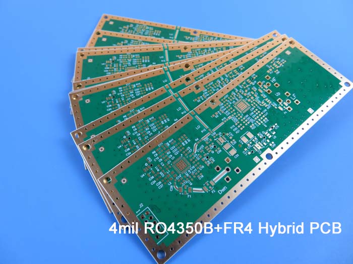
Hybrid PCB on Rogers RO4350B and High Tg FR-4 4-Layer Mixed PCB on 4mil RO4350B and 0.3mm FR-4
(PCBs are custom-made products; the images and parameters shown are for reference only)
Introduction
Hello Everyone,
Today, we will discuss a type of 4-layer high-frequency PCB constructed from 4mil RO4350B and high Tg FR-4 materials.
This PCB is designed as a 4-layer structure, making it relatively simple and cost-effective, which is beneficial for entering new markets.
Let's Explore the Build-Up
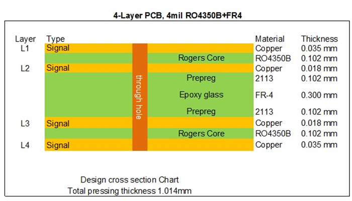
The first and second layers, as well as the third and fourth layers, consist of 4mil (0.102mm) RO4350B cores. This fixed thickness is crucial for maintaining the electrical length of the RF lines on the circuit board. The dielectric material in the middle is FR-4 epoxy glass, which bonds the cores on both the top and bottom sides. The inner layer copper weight is 0.5 ounces, while the outer layer is 1 ounce.
Detailed Specifications
Base Material |
RO4350B 0.102mm + Tg 170°C FR-4 0.30mm |
Layer Count |
4 layers |
Panel Size |
55mm x 132mm = 1 type = 1 piece |
Surface Finish |
Immersion gold |
Copper Weight |
Outer layer 35 μm / Inner layer 18 μm |
Solder Mask / Legend |
Green / White |
Final PCB Height |
1.0 mm |
Special Technology |
Via in pad (hole filled) under BGA |
Standard |
IPC 6012 Class 2 |
Packing |
25 panels are packed for shipment |
Lead Time |
12 working days |
Shelf Life |
6 months |
Applications
The applications for RO4350B hybrid PCBs are diverse, including:
Preamplifiers,Radar sensors,Digital transmitters,Splitter modules,GPS antennas,Communication relays,Analog transmitters,4G antennas,RF transmitters,Wi-Fi amplifiers,RFID systems,Attenuators
Advantages of RO4350B Hybrid PCBs
1)Stable Dielectric Constant: RO4350B maintains a consistent dielectric constant across a broad frequency range, making it ideal for broadband applications.
2)Improved Signal Integrity: Enhances performance compared to all-FR4 stack-ups.
3)Cost Efficiency: Reduces costs compared to stack-ups made entirely of low-loss materials.
4)Minimized Signal Loss: Effective at high frequencies.
5)Robust Capabilities: We meet your PCB requirements from prototypes to mass production, backed by certifications including IATF 16949 (2016), ISO 14001 (2015), ISO 9001 (2015), and UL certification for quality assurance.
Thank you for reading! Feel free to contact us for any inquiries regarding RF PCBs.
Appendix: Our PCB Capability 2022
Parameter |
Value |
Layer Counts |
1-32 |
Substrate Material |
RO4350B, RO4003C, RO4730G3, RO4360G2, RO4533, RO4534, RO4535, RO3003, RO3006, RO3010, RO3035, RO3203, RO3210; RT/Duriod 5880; RT/Duriod 5870, RT/Duriod 6002, RT/Duroid 6010, RT/duroid 6035HTC; TMM3, TMM4, TMM6, TMM10, TMM10i, TMM13i, Kappa 438; TLF-35; RF-35TC, RF-60A, RF-60TC, RF-35A2, RF-45, RF-10, TRF-45; TLX-0, TLX-6, TLX-7, TLX-8; TLX-9, TLY-3, TLY-5; PTFE F4B (DK2.2 DK2.65 DK2.85 DK2.94, DK3.0, DK3.2, DK3.38, DK3.5, DK4.0, DK4.4, DK6.15, DK10.2); AD450, AD600, AD1000, TC350; Nelco N4000, N9350, N9240; FR-4 ( High Tg S1000-2M, TU-872 SLK, TU-768, IT-180A etc.), FR-4 High CTI>600V; Polyimide, PET; Metal Core etc. |
Maximum Size |
Flying test: 900*600mm, Fixture test 460*380mm, No test 1100*600mm |
Board Outline Tolerance |
±0.0059" (0.15mm) |
PCB Thickness |
0.0157" - 0.3937" (0.40mm--10.00mm) |
Thickness Tolerance(T≥0.8mm) |
±8% |
Thickness Tolerance(t<0.8mm) |
±10% |
Insulation Layer Thickness |
0.00295" - 0.1969" (0.075mm--5.00mm) |
Minimum Track |
0.003" (0.075mm) |
Minimum Space |
0.003" (0.075mm) |
Outer Copper Thickness |
35µm--420µm (1oz-12oz) |
Inner Copper Thickness |
17µm--350µm (0.5oz - 10oz) |
Drill Hole(Mechanical) |
0.0059" - 0.25" (0.15mm--6.35mm) |
Finished Hole(Mechanical) |
0.0039"-0.248" (0.10mm--6.30mm) |
DiameterTolerance(Mechanical) |
0.00295" (0.075mm) |
Registration (Mechanical) |
0.00197" (0.05mm) |
Aspect Ratio |
12:1 |
Solder Mask Type |
LPI |
Min Soldermask Bridge |
0.00315" (0.08mm) |
Min Soldermask Clearance |
0.00197" (0.05mm) |
Plug via Diameter |
0.0098" - 0.0236" (0.25mm--0.60mm) |
Impedance Control Tolerance |
±10% |
Surface Finish |
HASL,HASL LF,ENIG,Immersion Tin,Immersion Silver, OSP, Gold Finger, Pure gold plated etc. |
